Rigid-Flex
PCB Built on FR-4 and Poyimide With Immersion Gold and 90ohm Impedance Control
(Flexible
printed circuits are custom-made products, the picture and parameters shown are
just for reference)
General
description:
It is also an impedance controlled design on outer layers and inner
flexible circuit. Immersion gold is plated on pads for latter SMT. The base
laminate is from Shengyi, It’s fabricated per IPC 6012 Class 2 using supplied
Gerber data.
Parameter
and data sheet:
|
Size of
Flexible PCB
|
20.61 X 50.17mm
|
|
Number of Layers
|
6
|
|
Board Type
|
Rigid flex PCB
|
|
Board Thickness
|
1.4mm
|
|
Board Material
|
FR-4
/ Polyimide
|
|
Board Material Supplier
|
Shengyi
|
|
Tg Value of Board Material
|
130℃
|
|
|
|
PTH Cu thickness
|
≥20 µm
|
|
Inner Iayer Cu thicknes
|
18
µm
|
|
Surface Cu thickness
|
35
µm
|
|
|
|
|
Coverlay Colour
|
Yellow
coverlay / Green solder mask
|
|
Number of Coverlay
|
2
|
|
Thickness of Coverlay
|
25
µm
|
|
Stiffener Material
|
N/A
|
|
Stiffener Thickness
|
N/A
|
|
|
|
|
Type of Silkscreen Ink
|
IJR-4000
MW300
|
|
Supplier of Silkscreen
|
TAIYO
|
|
Color of Silkscreen
|
White
|
|
Number of Silkscreen
|
1
|
|
|
|
Peeling test of Coverlay
|
No
peelable
|
|
Legend Adhesion
|
3M 90℃No
peeling after Min. 3 times test
|
|
|
|
Surface Finish
|
Immersion
Gold
|
|
Thickness of Nickle/Gold
|
Au:
0.03µm(Min.); Ni 2-4µm
|
|
RoHS Required
|
Yes
|
|
Famability
|
94-V0
|
|
|
|
Thermal Shock Test
|
Pass, -25℃±125℃, 1000 cycles.
|
|
Thermal Stress
|
Pass, 300±5℃,10 seconds, 3 cycles. No delamination, no blistering.
|
|
Function
|
100%
Pass electrical test
|
|
Workmanship
|
Compliance
with IPC-A-600H & IPC-6013C Class 2
|
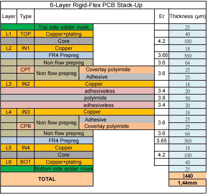
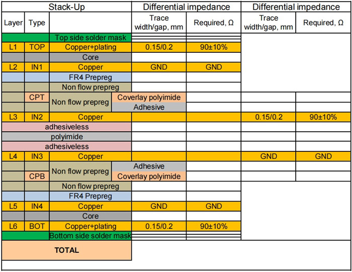

Features
and benefits:
Excellent
flexibility
Reducing
the volume
Weight
reduction
Consistency
of assembly
Increased
reliability
The
end can be whole soldered
Low
cost
Continuity
of processing
No
minimum order quantity and low cost sample.
Make
delivery on time. We keep higher than 98% on-time-delivery rate.
Applications:
Contact
belt of inkjet printer, industrial surveying and mapping instrument, Tablet PC
camera soft board
Flexible
Inner Layers:
Inner
layers are produced as single- or double-sided flexible circuits in the same
way i.e., imaged, etched and covercoated, but not drilled and plated.
Covercoating of the individual inner layer circuits requires an extra process,
but the advantage is less risk of air entrapment.
The
inner layers in the flexible section can also be bonded together . Although it
is a simpler design that involves fewer process steps, the finished circuit has
the disadvantage of being fairly rigid, and therefore difficult to bend. This
is reflected in a rather limited number of bend cycles, e.g., maximum 25.
Another
method is to avoid bonding of the flexible circuits in the flexible area. In
the case of many inner layers, or when there is a short distance between the
rigid sections of a flex/rigid circuit, a staggered build-up can be employed.
This prevents buckling of the individual layers when the circuit is to be bent
into its installed position, but the manufacture is somewhat more complicated.
Rigid
Outer Layers:
In
the case of flex/rigid circuits, rigid materials such as FR-4 are cut to size,
and bonded to the circuit in the lamination process. It is possible to produce
the flex/rigid circuit as a temporarily rigid board to facilitate handling
during manufacture, assembly and soldering. This is achieved by extending the
rigid layers across the flexible section. By covering both sides of the
flexible section with release films, bonding of the rigid outer layers to the
flexible section is prevented. The non-bonded sections of the rigid material
can be removed by a snap-action, provided grooves are cut before lamination at
the interfaces in both sides of each rigid outer
layer.
Processes:
A
simplified flow diagram is shown below.

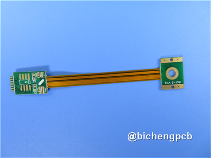
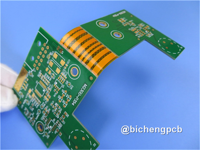
More
Displays of rigid-flex PCB:
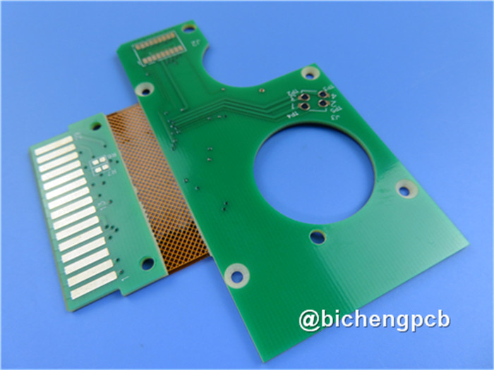
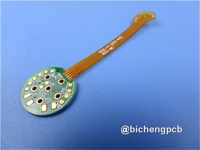
BICHENG PCB WORKSHOP:
BICHENG PCB CERTIFICATE:
BICHENG MAIN COURIERS:
